


Description
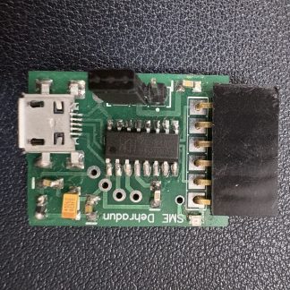
NuttyFi 2.0 is an advanced Wi‑Fi IoT development board built around the ESP8266 module. It’s designed to help you prototype, research, and ship production‑ready connected products—from automation and sensing to dashboards and data logging. Program it with the Arduino IDE or your preferred toolchain and deploy quickly.
Core idea: a compact, open, Arduino‑like, USB‑powered Wi‑Fi/serial transceiver board that lets you monitor, manage, and control devices from anywhere worldwide.
To install the NuttyFi IoT Board in Arduino IDE, follow below step-by-step guide:
Boards Manager URL (go to Arduino IDE → Preferences → Additional URLs):
Arduino Board Manager URL:
https://raw.githubusercontent.com/itsbhupendrasingh/Nuttyfi/main/package/package_nuttyfi_index.json
Tip: Arduino IDE supports multiple Additional URLs. Put each on a new line (IDE 2.x) or separate with commas (IDE 1.8.x).
NuttyFi2.0 Customised IoT Board
A compact, high-performance IoT development board designed for makers, students, and professionals. Now featuring dedicated 5V, 3.3V, and GND pins for easy sensor integration, a sleek PCB layout, and a standalone lightweight board manager for faster development.
Everything you need — nothing you don’t.
Standalone Board Manager Package:
NuttyFi 2.0 comes with its own minimal Board Manager file containing only the NuttyFi board—no extra boards, no bloat.
What’s New in NuttyFi 2.0:
Dedicated 5V, 3.3V & GND Expansion Pins:
Easily connect sensors and external modules directly—no additional breakout boards required.Sleeker & Lighter Hardware Design:
A more compact and refined layout compared to bulky ESP8266 development boards.- Faster & Lighter Development Environment:
Because the Board Manager package is lean, it keeps your Arduino IDE/software lightweight and prevents the slowdowns caused by bulky ESP8266 packages.Optimized for Clean & Hassle-Free Development:
Install, compile, and upload faster with a streamlined toolchain designed specifically for NuttyFi.
Why NuttyFi2.0?
Plug-and-Play Sensor Expansion
With dedicated 5V, 3.3V, and GND pins, adding sensors and modules is easier than ever.Compact, Sleek & Efficient
A redesigned and refined PCB reduces clutter and improves usability.Lightweight Board Manager
No extra boards. No unnecessary files. Just NuttyFi—fast and clean.Built for Stability
Improved power routing ensures reliable operation even with multiple modules attached.
Perfect for:
IoT Products, IoT prototyping, home automation, student projects, sensor networks, and lightweight WiFi-based applications.
Power Option:
- USB 5 V (Micro‑B) → on‑board 3.3 V LDO. Ideal for development & uploads.
- VIN → on‑board regulator to 3.3 V. (Populate and heatsink as needed.)
Important: Provide at least 600 mA burst capacity on 3.3 V to avoid brown‑outs during Wi‑Fi TX. Keep antenna area clear of ground copper/enclosures.


Reviews
There are no reviews yet.